Abstract
Artificial Intelligence (AI) is increasingly influencing printed circuit board (PCB) design by enhancing traditional electronic design automation (EDA) workflows with predictive analytics, automation, and data-driven decision-making. From schematic development to layout optimization and manufacturability validation, AI-driven tools are helping reduce design cycles, improve first-pass success, and support higher design complexity. This article highlights key application areas of AI in PCB development and discusses implications for designers, manufacturers, and IPC standards alignment.
Why AI Matters in PCB Design
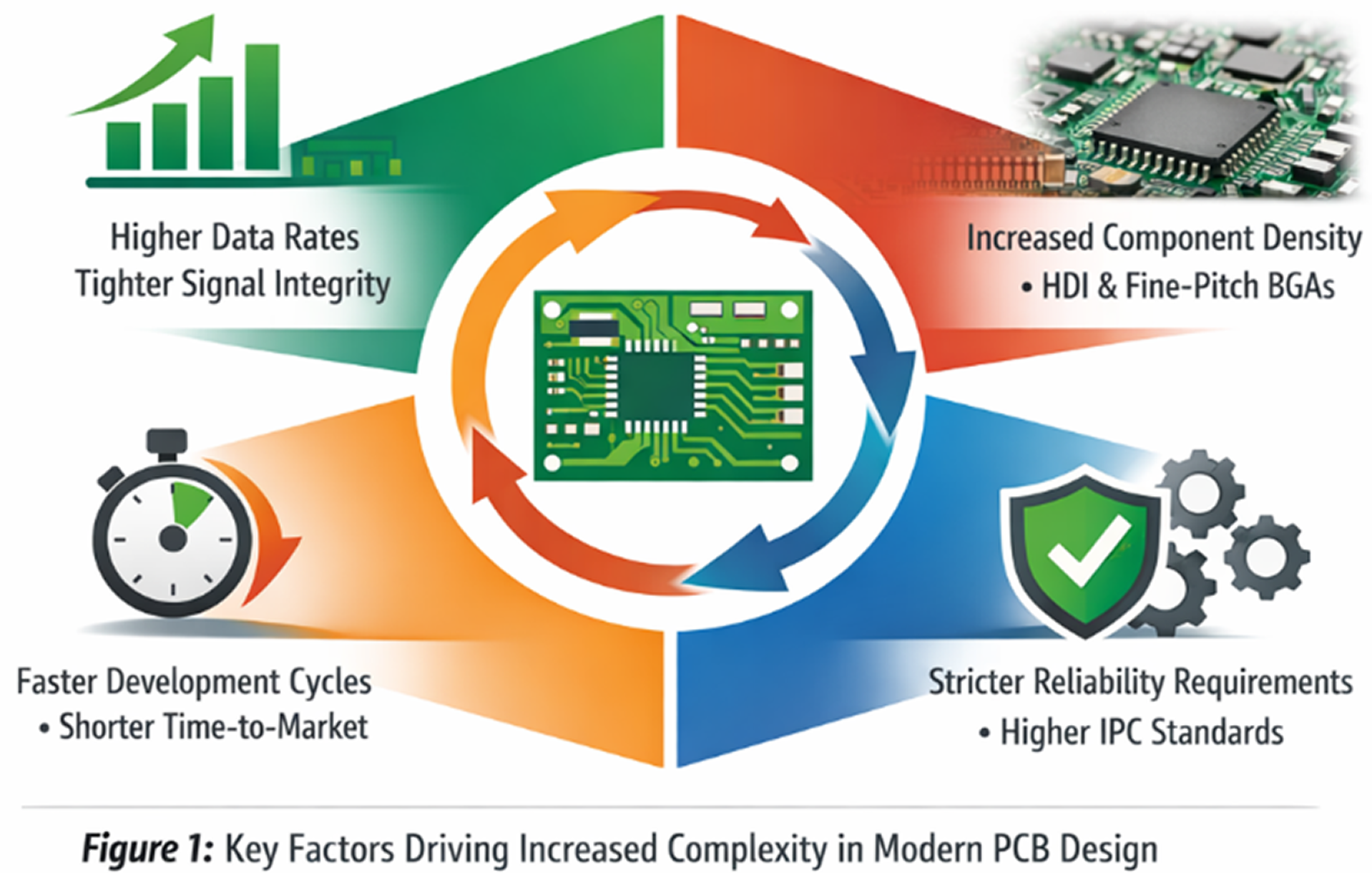
PCB designers today face growing challenges: higher data rates, tighter signal-integrity margins, increasing component density (HDI and fine-pitch BGAs), shorter development cycles, and stricter reliability expectations.
Conventional rule-based EDA tools depend heavily on designer experience and multiple manual iterations.
AI-driven design tools address these challenges by analysing large volumes of historical design, manufacturing, and failure data, enabling potential risks to be identified much earlier in the design process .
What Is AI-Driven PCB Design?
AI-driven PCB design combines machine learning, generative design, and predictive analytics to optimize design decisions within defined electrical, mechanical, and manufacturing constraints.
Unlike traditional automation, AI systems continuously improve as more design and production data is incorporated, resulting in increasingly accurate recommendations over time.
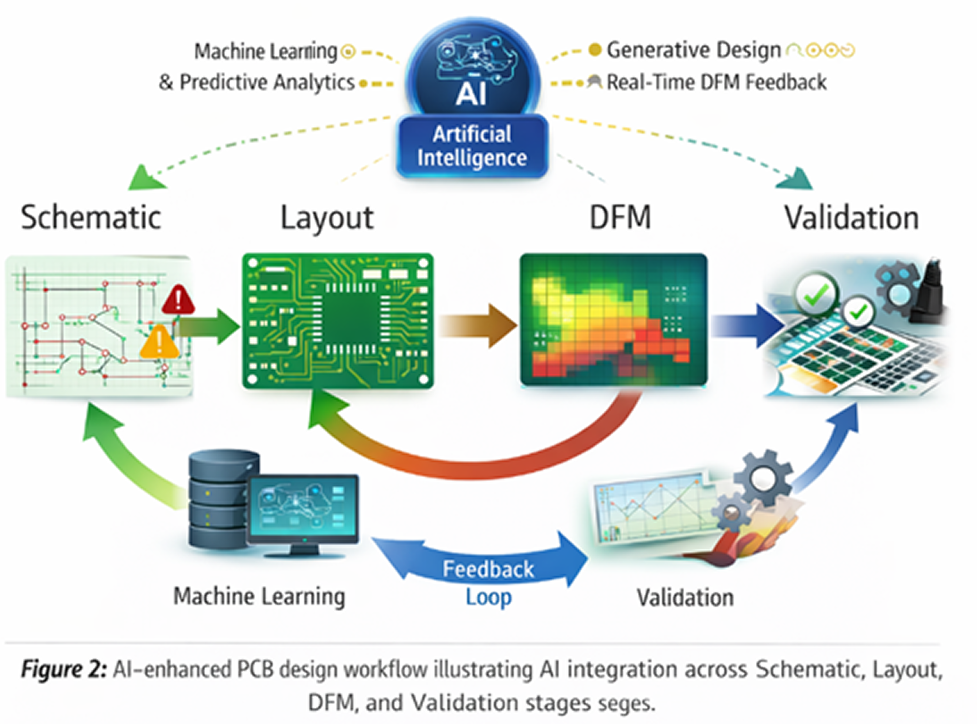
Key Areas of Impact
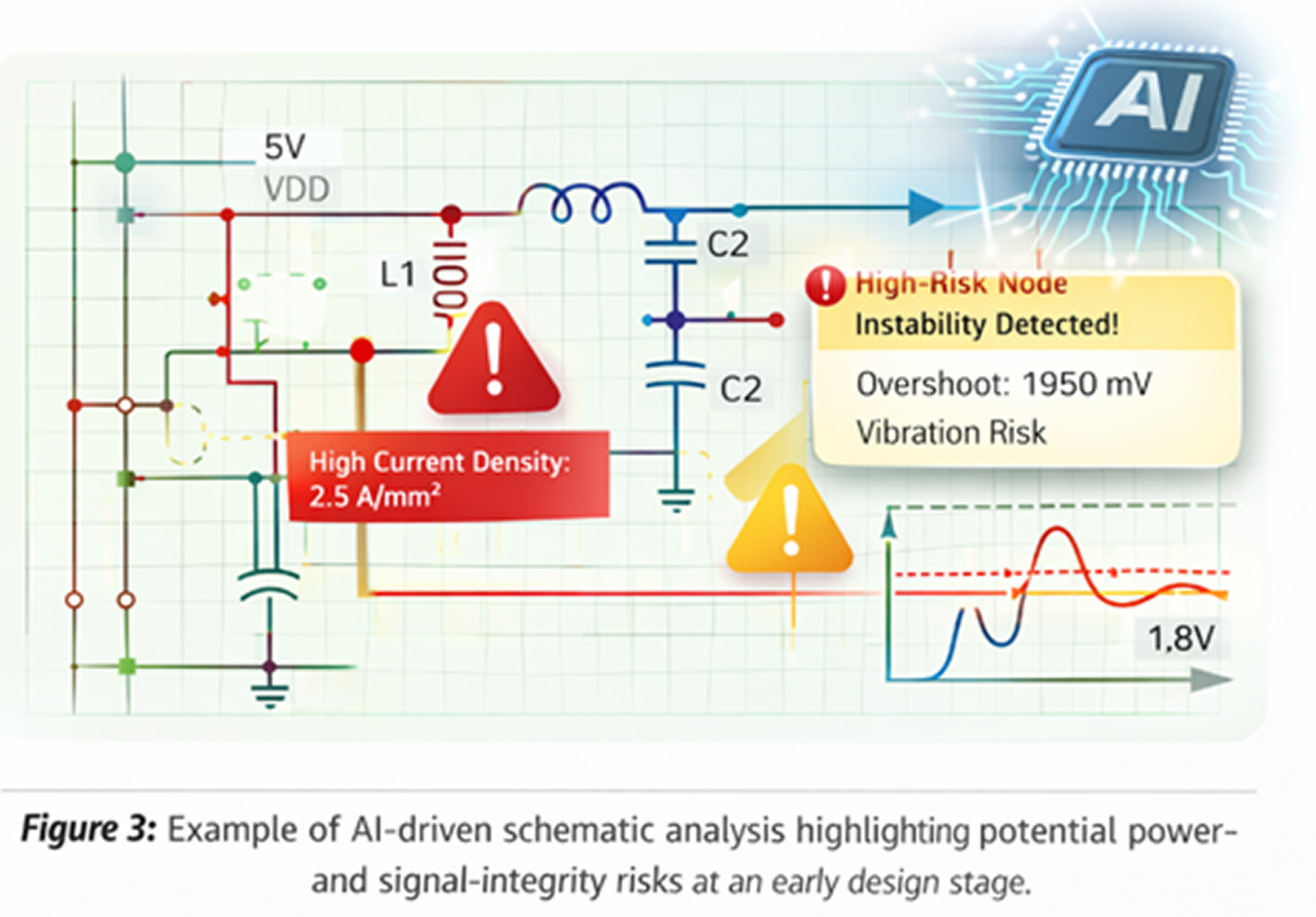
Intelligent Schematic Development
AI-assisted schematic tools can flag high-risk circuit topologies, predict power- and signal-integrity concerns, and suggest component alternatives based on availability and lifecycle status.
By addressing these issues early, designers can significantly reduce downstream layout rework.
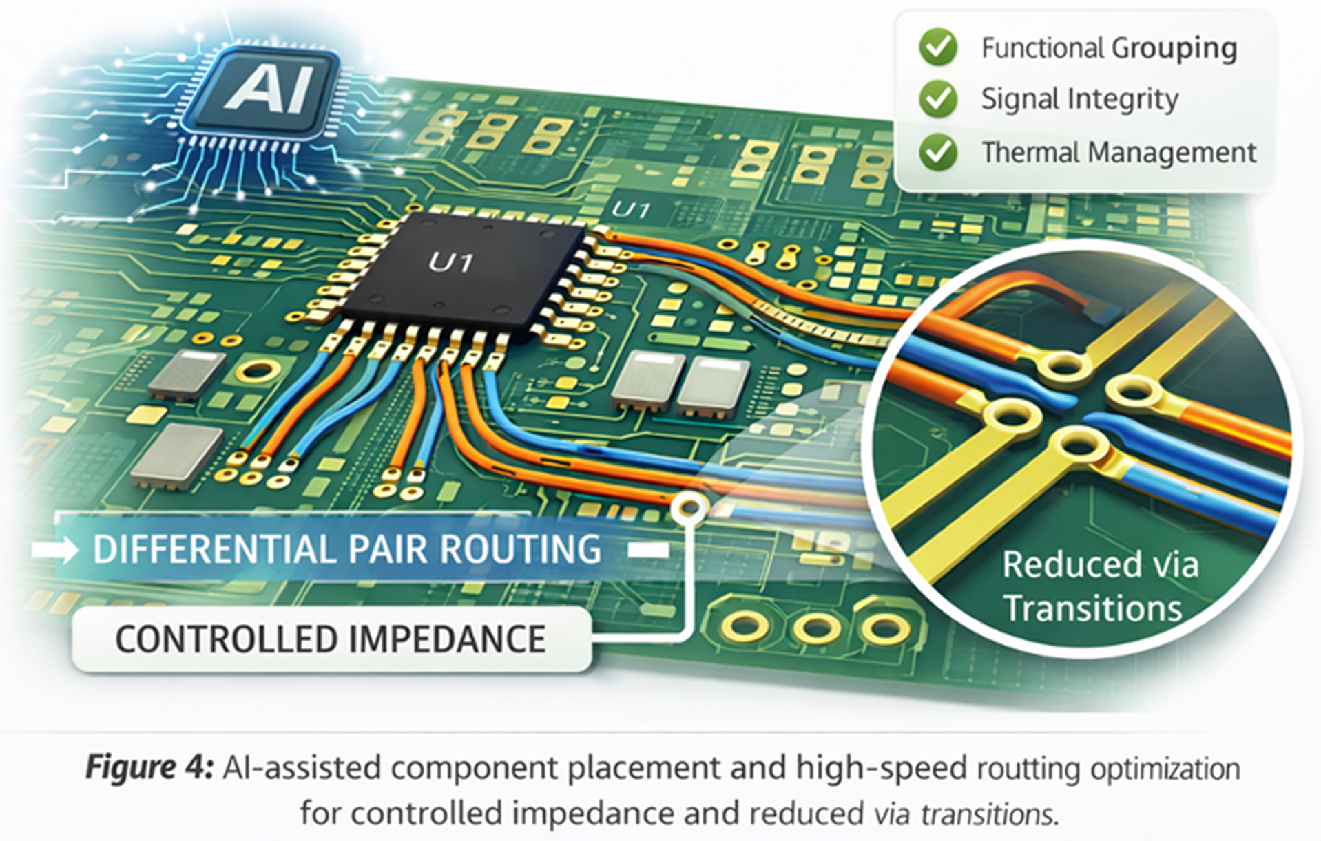
AI Layout and Routing
AI-based layout engines support automated component placement based on functional grouping, thermal behavior, and signal flow. Routing optimization considers impedance control, length matching, and EMI reduction, while learning from previously successful designs.
In high-speed applications, AI can automatically propose optimized differential-pair routing with minimal via transitions, improving signal integrity and reducing iteration cycles
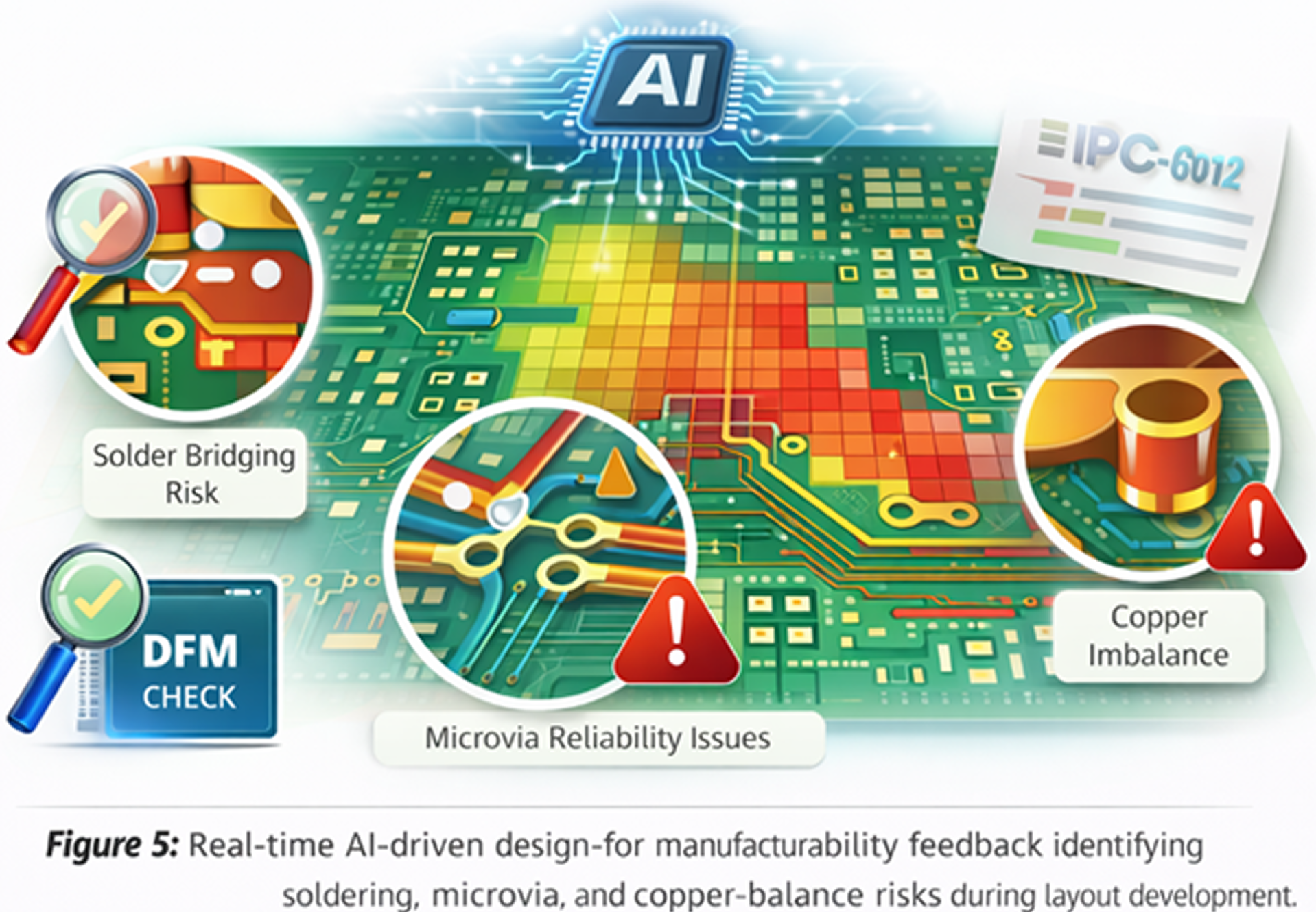
Design for Manufacturability (DFM) Prediction
One of the most valuable applications of AI is real-time manufacturability prediction. AI systems can identify recurring production risks such as solder bridging, microvia reliability issues, copper imbalance, and warpage tendencies.
Instead of relying solely on post-layout DFM checks, designers receive continuous feedback during layout development.
This approach supports early alignment with IPC-2221 design intent and fabrication capability requirements defined in IPC-6012 .
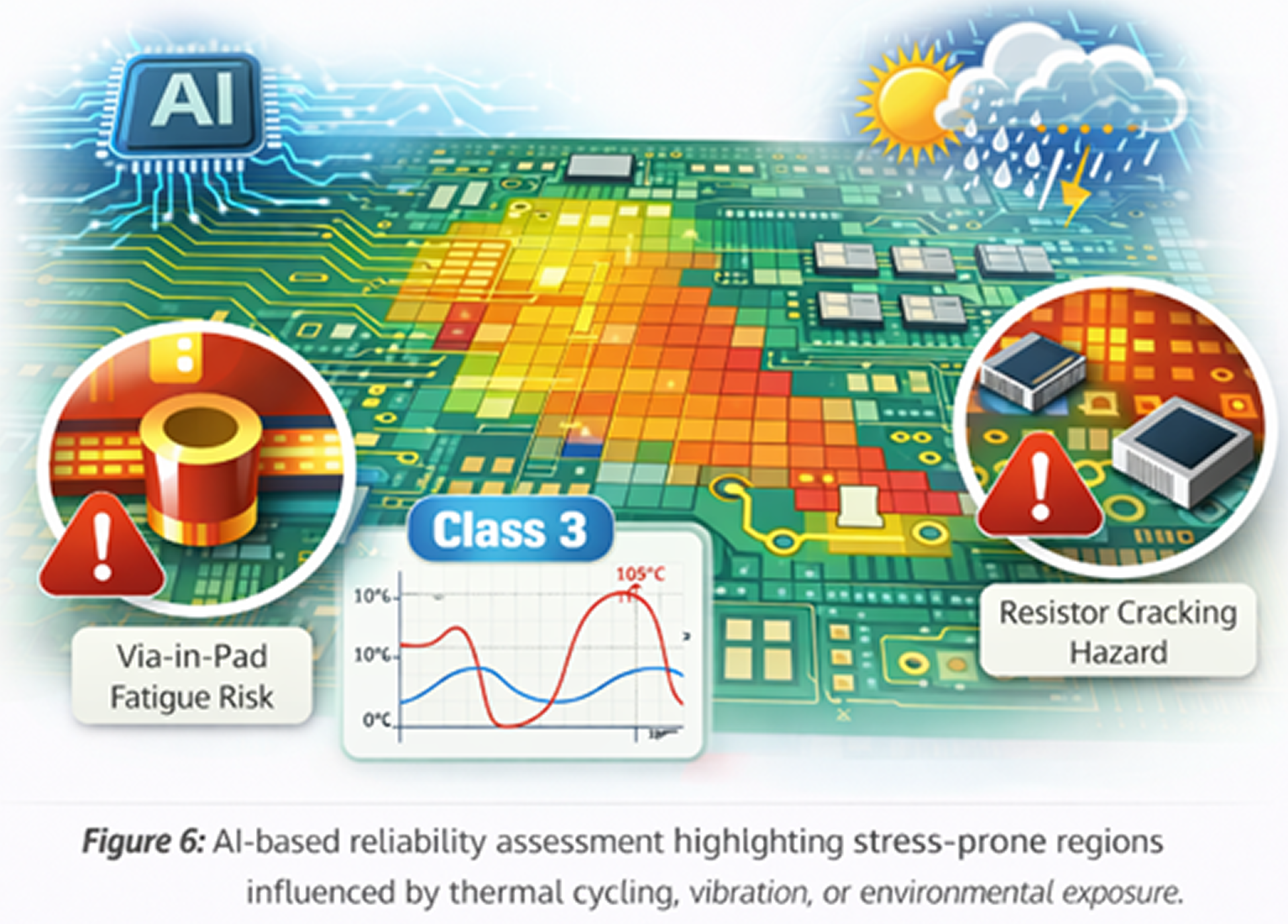
Reliability and Lifecycle Optimization
AI models trained on field-return and reliability data can predict long-term failure risks and identify stress-prone areas related to thermal cycling, vibration, and environmental exposure.
For high-reliability applications, such as IPC Class 3 products, AI can highlight design features with elevated fatigue or reliability risk, enabling corrective action before production.
Design Cycle Time Reduction
By reducing trial-and-error iterations, AI-assisted workflows lower the number of layout revisions and engineering change orders. Many organizations report development cycle reductions of 20–40%, along with improved first-pass yield, when AI tools are effectively integrated into existing EDA environments.
Human Expertise and AI: A Collaborative Model
AI does not replace PCB designers. Instead, it enhances engineering judgment by automating data-intensive tasks and presenting informed design recommendations.
Human expertise remains essential for interpreting trade-offs, addressing customer-specific requirements, and ensuring correct application of IPC standards.
Challenges and Future Direction
Key challenges include data quality, trust in AI-generated recommendations, and integration with legacy EDA tools. From an IPC perspective, future considerations include how AI-driven decisions can be validated against established standards and acceptance criteria.
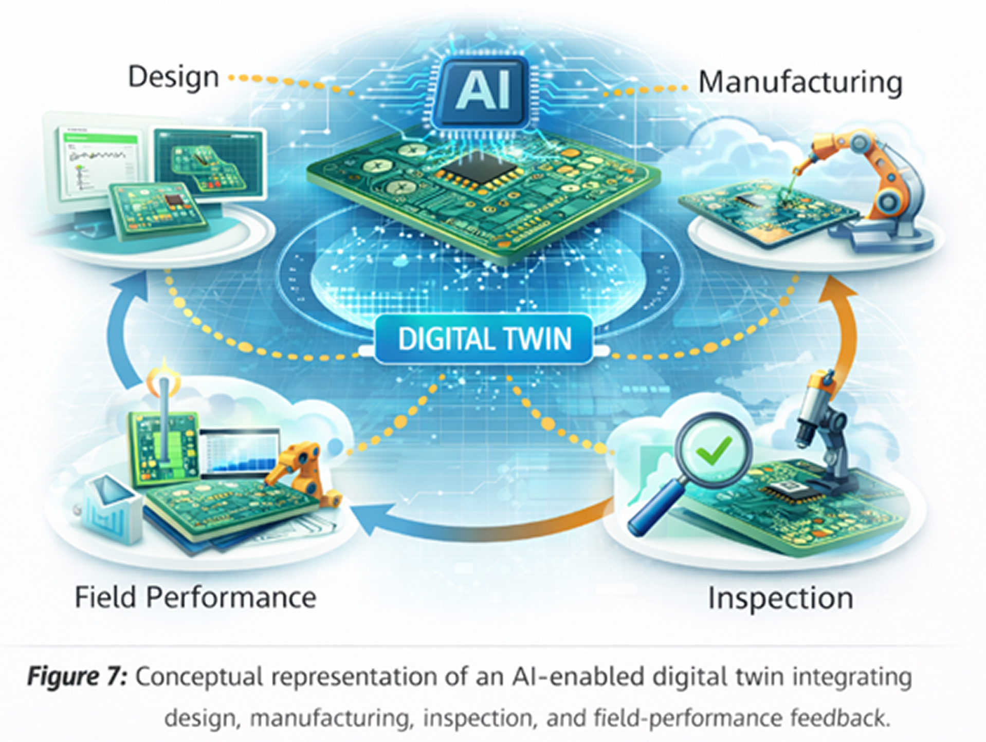
Looking ahead, AI-driven PCB design is evolving toward digital twins, closed-loop feedback from manufacturing and inspection, and predictive compliance with IPC requirements
Conclusion
AI-driven design tools are reshaping PCB development by enabling faster, more reliable, and more manufacturable designs. When combined with sound engineering judgment and IPC standards knowledge, AI becomes a powerful enabler of right-first-time design success.