Supported by

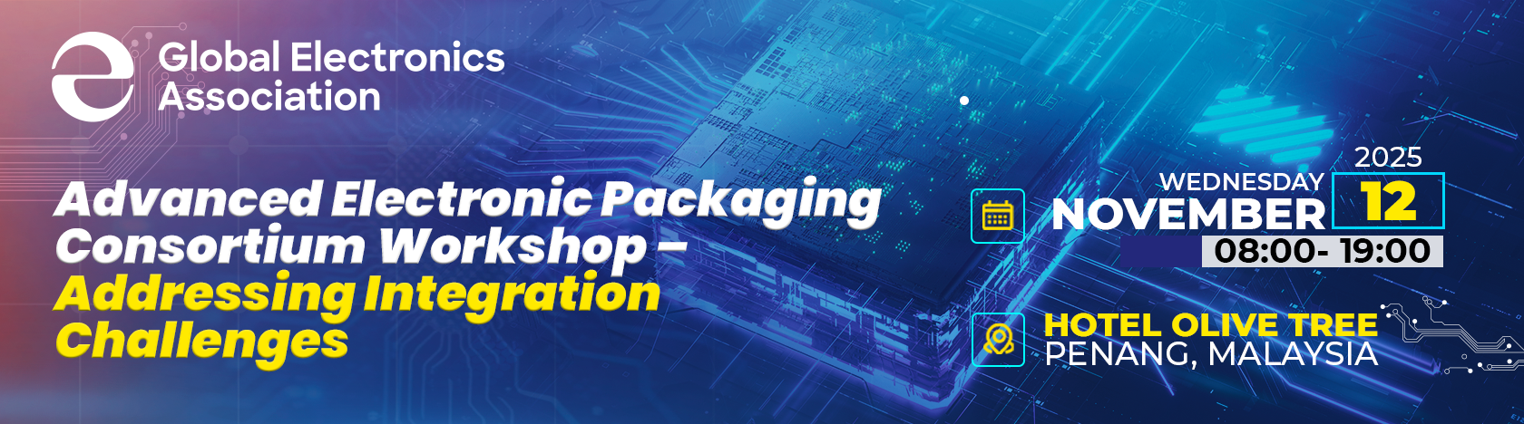
 Venue
Venue
Hotel Olive Tree Penang, 76, Jalan Mahsuri, Bandar Sunway Tunas,
11950 Bayan Lepas, Penang, Malaysia
Program Schedule
08:15 | Registration and Morning Coffee |
09:05 | Welcome, Scope and Introduction |
09:15 | Workshop Intent and Expectations Bernard Lim, Advisor Advanced Packaging Technology, Global Electronics Association |
09:25 | "Global Electronics Association - Introduction, Focus Areas, Collaboration" Ranee Ramya, Country Manager, Malaysia, Global Electronics Association |
09:50 | Advancing the National Semiconductor Strategy: From Vision to Action Speaker: Mr Lau Yue Hoong, CREST |
10:10 | Introduction to Advanced Packaging Consortium Speaker: Mr. ET Tan, Malaysia Advance Packaging Consortium (MAPC) |
10:40 | Morning Tea break |
11:00 | Unlocking Malaysia’s Semiconductor Potential: Advanced Packaging as the Next Frontier Speaker: Dr Siti Fatimah Binti Kamarudin, MIMOS Berhad |
Track 1 | Design Needs and Advanced Electronics Packaging Challenges |
11:20 | Enabling Tomorrow’s Packaging: Skyechip’s Test Chip Solutions for Advanced Electronic Integration Speaker: Mr Teoh Giap Seng, SkyeChip |
11:40 | From Semiconductors to Electronics: The Manufacturing Path from Wafers to Systems Speaker: Mr Ooi Teng Chow, FusionAP |
12:00 | Driving Semiconductor & Photonics Innovation: Chip-to-System Integration Speaker: Mr S Satish, CADFEM Malaysia |
12:20 | Panel: SkyeChip,FusionAP, CADFEM Moderator: Dr Devan Iyer, Mr Matt Kelly |
13:00 | Networking Lunch |
Track 2 | Advanced Electronics Packaging Materials, Assembly & Manufacturing |
14:15 | "Malaysia’s Advanced Packaging Transition: From OSAT Strength to Heterogeneous Integration Leadership" Speaker: Sabran, Inari Technology Sdn Bhd |
14:35 | "Novel Interconnect Materials Enabling Heterogeneous Integration" Speaker: Lim Sze Pei, Indium Corp |
14:55 | Trends & Challenges in Large Body Package Assembly to Printed Circuit Boards Speaker: Mr. Nadarajan, Flextronics |
15:15 | Tea break |
15:35 | Panel Session: Inari Technology, Indium, Flextronics, NXP Moderator: Mr Allen Cheah |
Track 3 | Advanced Electronics Packaging Tests and Reliability |
16:15 | Automation and Intelligence in Advanced Packaging - Approach to AI-Ready Assembly Solutions Speaker: Mr Teoh Siow Khiang, Pentamaster |
16:35 | Precision and Reliability in Assembly Solutions for Next‑Gen Advanced Electronic Packaging Speaker: Mr KN Boo, NSW |
16:55 | "Enabling Future AI Era with Advanced Chip/Chiplet interconnect for 2.5D and 3D Packaging" Speaker: Mr Eric Ng, ASMPT |
17:15 | Panel Session: Pentamaster, NSW, ASMPT Moderator: Dr Bernard Lim |
17:55 | Social Event – Networking |
Advanced electronic packaging is a vital technology that enables the integration of high density, high speed and high-power electronic devices in small form factor packages and modules. As technologies constantly evolve in areas like Artificial Intelligence (AI), 5G/6G, Electric and Autonomous vehicles, and the Internet of Things (IoT), legacy packaging technologies need to be transitioned to advanced packaging.
Advancements in compute and storage for automotive applications, sensor technologies with mmWave Radar, LIDAR, and other sensing techniques along with integrated power systems for EV with high voltage, high power components and modules are bringing new challenges to both, Component-Level Packaging (CLP) and Printed Circuit Board Assembly /System-Level-Packaging (SLP). Power delivery, thermal management, assembly and reliability at component/system level demand innovative design approaches, materials and assembly processes for high reliability automotive and industrial requirements.
Chip to package interaction at the component level packaging and package to board interaction at the system level packaging are indispensable from system level integration and final product/system performance points of view. With heterogenous integration solutions and miniaturization, the some of the components from the board are moving inside the package creating System-in-Package (SiP) solutions.
Investing in advanced packaging will support the growth in an industry. A stronger semiconductor ecosystem will encourage the growth of local small and medium-sized enterprises (SMEs), researchers and faculty members in universities, and research centres, promoting innovation and new knowledge development and transfer. This will make Malaysia more self-reliant and resilient against global supply chain disruptions. These applications demand significant system miniaturization through complex chiplet concepts and heterogenous integration solutions for processors, memories, power management along with sensors and MEMS, wireless and optical connectivity and other advanced communication components and systems.
This workshop is intended to bring together Government officials, industry experts, academic faculty members from universities presenting and discussing components and system level packaging trends, challenges, possible paths to solutions and the needs for developing guidelines/ standards desired for design, assembly, test, reliability and manufacturing. This workshop is also intended to discuss R&D focus areas and knowledge enhancement needs for local companies in semiconductor and system level packaging and how to work collaboratively in a Consortium environment.
Free Registration: Click here
Workshop Sponsorship: Click here
For more information, please connect with:
Dr. Ranee Ramya
Country Manager - Malaysia
raneeramya@electronics.org