Detex Corporation of New Braunfels, Texas—like many companies—strives to cultivate a highly skilled workforce to meet the growing demand for electronics assembly professionals. However, as with many in the industry, hiring qualified workers has been a persistent challenge. Most employees arrive without certification or prior experience, and providing on-the-job training (OJT) without structured technical instruction has seen limited success.
So when Martha Rodriguez, Human Resources Manager at Detex, met Coreen Blaylock, Director of Workforce Partnerships at the Global Electronics Association, she immediately recognized the potential of adopting an apprenticeship model to upskill employees efficiently and with minimal downtime.
Building a Workforce Through Apprenticeships
After adopting the apprenticeship model, Victoria Hawkins, the Association’s Director of Workforce Grants and Proposals, helped Detex secure $375 per apprentice—totaling $7,500 for 20 apprentices—along with $10,000 for technical instruction. The company also anticipated an additional $180,000 grant from the Texas Workforce Commission to cover translation services, supplies, and Certified Instructor Trainer (CIT) training.
“Victoria’s patience and expertise were crucial in completing the grant application,” says Rodriguez. “She provided a detailed outline of the apprenticeship program, funding requirements, and step-by-step guidance. Her support made it possible to launch our onsite apprenticeship program in early March 2024.”
Addressing Business Goals Through the Registered Apprenticeship Program
Martha Rodriguez: “Our goal is to reduce the ongoing recruiting challenges as we compete with other employers for qualified assemblers from the same talent pool. The Registered Apprenticeship Program (RAP), tailored for electronics assemblers, meets the needs of our growing manufacturing sector—especially here at Detex. It directly supports our demand for skilled workers.”
Benefits for Both the Company and Its Employees
“With the onsite apprenticeship program, we can upskill our current workforce quickly, train new hires effectively, and increase skill levels—all of which improve compensation and retention,” says Rodriguez.
The program provides a structured career progression, empowering employees to advance through self-paced OJT designed for professional growth. It supports economic stability and retention, while creating a certified soldering talent pipeline within the company.
Using Funding for Training and Development
Detex has developed partnerships with Texas State Technical College (TSTC), the local chamber of commerce, and workforce development agencies to deploy the Association’s comprehensive electronics assembler apprenticeship curriculum—customized to meet Detex’s specific needs.
Employees and local job seekers receive both theoretical and practical instruction, ensuring apprentices gain the knowledge and skills needed to excel. Funding from the Global Electronics Association offsets related technical instruction costs, reducing turnover and improving operational efficiency.
Industry-Recognized Certifications
Through the program, apprentices earn two credentials:
- Global Electronics Association Soldering Certification
- Journey-worker Certification issued by the U.S. Department of Labor
These credentials come without external tuition costs, allowing employees to advance without financial strain. “By investing in our people,” Rodriguez notes, “we’re not just building skills—we’re building career pathways and positioning Detex as an employer of choice.”
Expanding the Apprenticeship Program
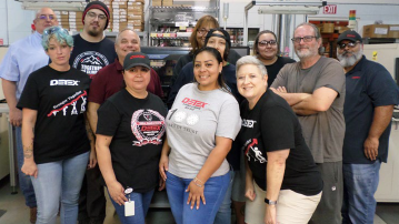
The first cohort included 27 apprentices starting in March, with 20 completing Level 1 online training and moving into hands-on production. Another 20 employees are expected to join later in the year. The workforce is diverse—largely women, many over 40, and from a variety of backgrounds.
Partnering with Local Schools
Detex also works with local high schools to strengthen the talent pipeline. Students interested in manufacturing can now take relevant classes and participate in pre-apprenticeship training to prepare for the workforce. Schools plan to send Career Technical Education (CTE) teachers for CIT training, supporting Manufacturing and Electrical Systems certification pathways.
This collaboration not only benefits students by enhancing College, Career, and Military Readiness (CCMR) but also gives Detex access to a future-ready workforce.
The Importance of Community Partnerships
“As HR Manager, I believe partnering with organizations that support employee development and recruitment is key to our success,” Rodriguez says.
In addition to working with the Global Electronics Association, TSTC, and local industry leaders, Detex partners with the Texas Workforce Commission, which coordinates educational training and hiring efforts. This collaboration builds a pipeline of qualified new hires ready to enter manufacturing roles.
The Value of Collaboration
Each partnership plays a vital role. Detex plans to train two to three Certified Global Electronics Association Trainers (CITs) to certify apprentices locally—saving the cost and difficulty of sending employees to distant training centers.
TSTC is also training its instructors to become CITs, ensuring students graduate already certified and job-ready. Together, these partnerships are strengthening the local manufacturing ecosystem.
About Detex Corporation
Detex designs, engineers, and manufactures security products—including door hardware, turnstiles, and electronic systems for facilities such as retail stores, hospitals, schools, and airports. The company has recently expanded production capabilities to build circuit boards in-house, reducing reliance on outsourcing and increasing control over quality.