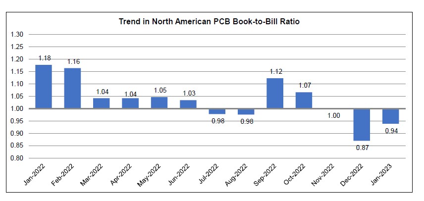
EMS North America Industry Report, May 2022

IPC releases EMS industry results for May 2022

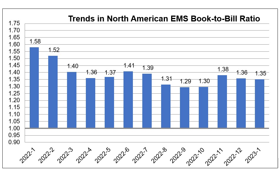
IPC announced today the May 2022 findings from its North American Electronics Manufacturing Services (EMS) Statistical Program. The book-to-bill ratio stands at 1.35.

Total North American EMS shipments in May 2022 were up 9.4 percent compared to the same month last year. Compared to the preceding month, May shipments rose 0.6 percent.

EMS bookings in May increased 7.0 percent year-over-year and decreased 6.8 percent from the previous month.

“Recent results for the EMS industry continue to suggest strained supply chains. Orders have grown 11.2 percent, outpacing shipment growth of 7 percent,” said Shawn DuBravac, IPC’s chief economist. “The book-to-bill has moderated from last year's highs but remains elevated as businesses continue to work on key components.”

EMS book to bill ratio chart May 2022

Detailed Data Available

Companies that participate in IPC’s North American EMS Statistical Program have access to detailed findings on EMS sales growth by type of production and company size tier, order growth and backlogs by company size tier, vertical market growth, the EMS book-to-bill ratio, 3-month and 12-month sales outlooks, and other timely data.

Interpreting the Data

The book-to-bill ratios are calculated by dividing the value of orders booked over the past three months by the value of sales billed during the same period from companies in IPC’s survey sample. A ratio of more than 1.00 suggests that current demand is ahead of supply, which is a positive indicator for sales growth over the next three to twelve months. A ratio of less than 1.00 indicates the reverse.

Year-on-year and year-to-date growth rates provide the most meaningful view of industry growth. Month-to-month comparisons should be made with caution as they reflect seasonal effects and short-term volatility. Because bookings tend to be more volatile than shipments, changes in the book-to-bill ratios from month to month might not be significant unless a trend of more than three consecutive months is apparent. It is also important to consider changes in both bookings and shipments to understand what is driving changes in the book-to-bill ratio.

IPC’s monthly EMS industry statistics are based on data provided by a representative sample of assembly equipment manufacturers selling in the USA and Canada. IPC publishes the EMS book-to-bill ratio by the end of each month.

The Keys to 100% Effective Reliability Testing and Failure Analysis of HDI/Microvias

Member Download (pdf)

The move from Plated Through Vias (PTVs) to advanced HDI interconnects is challenging the electronics industry, not only due to the increased complexity of design and manufacturing, but even more due to the difficulties associated with screening and testing at every level: PWB, assembly, and system. Unlike PTVs there is no definitive cross-section quality criteria to tell good from bad, testing requires very specific conditions to detect fine separations caused by reflow, the high variation in failure response challenges typical sampling plans, and even known failures can be very difficult to locate electrically and/or in an x-section.

This paper uses examples from over 25 years of testing advanced interconnects including microvias to show not only how they fail but more importantly how a unique attribute of their failure curves can be used to advantage to assure reliable product in any operational environment. The importance of peak test temperature with sufficient dwell, continuous resistance monitoring, coupon design, coupon location, thermal profile, and choice of failure criteria is demonstrated. The Temperature Coefficient of Resistance (TCR) Measurement is explained as both a foundation for thermal cycling tests and an informative test in itself. IPC methods 2.6.26B, 2.6.27A, and 2.6.7.2 are compared, with recommendations to improve effectiveness. Finally, a simple approach to locate and x-section microvia failures every time is presented.

Author(s)
Kevin Knadle
Resource Type
Technical Paper
Event
IPC APEX EXPO 2020

IPC APEX EXPO 2023 Call for Participation Deadline Extended

Abstracts due August 8

IPC has extended the deadline for IPC APEX EXPO 2023 technical conference and professional development abstracts to Monday, August 8, 2022. The IPC APEX EXPO 2023 technical conference will take place January 24-26 and professional development courses will run from January 21-26.

“Our Technical Program Committee members received multiple requests from authors for more time to prepare and submit abstracts, and we are happy to accommodate by extending our deadline for abstract submission,” said Julia Gumminger, manager, IPC professional development and events. “We look forward to seeing the exciting new work from our colleagues in the global electronics manufacturing industry.” 

The industry’s premier conference and exhibition for electronics manufacturing in North America, IPC APEX EXPO provides presenters and their companies with a notable and cost-effective opportunity to promote their expertise and gain visibility with key engineers, managers, and executives from all segments of the industry worldwide.

For technical conference paper presentations and posters, IPC seeks abstracts that describe significant results from research experiments, highlight new techniques or materials, and/or discuss cutting-edge trends and challenges facing the electronics manufacturing industry. Conference speakers are entitled to a free one-day conference pass for the day of their presentations. Papers will be published in a proceedings document, and both paper and poster presentations will be delivered in person at IPC APEX EXPO 2023 in San Diego.                            

To recognize exceptional achievement, the IPC Technical Program Committee will select top qualifying papers and one top poster for awards. Awards include “Best of Conference,” “NextGen Best Paper,” “Best Student Research Paper,” and “Best Technical Poster.” 

For professional development courses, IPC seeks abstracts for three-hour sessions of live instruction covering all aspects of electronics manufacturing. Courses can be offered as one 3-hour session or two 3-hour sessions (offered as Part 1 & Part 2 for a total of 6 hours). Honoraria and travel expense stipends are offered to professional development instructors.

To submit an abstract, visit www.ipcapexexpo.org/CFP. For more information on IPC APEX EXPO 2023, visit www.ipcapexexpo.org.

High-Density PCB Technology Assessment for Space Applications

Member Download (pdf)

High density interconnect (HDI) printed circuit boards (PCBs) and associated assemblies are essential to allow space projects to benefit from the ever increasing complexity and functionality of modern integrated circuits such as field programmable gate arrays (FPGAs), digital signal processors (DSPs) and application processors. Increasing demands for functionality translate into higher signal speeds combined with an increasing number of I/Os. To limit the overall package size, the contact pad pitch of the components is reduced. The combination of a high number of I/Os with a reduced pitch places additional demands onto the PCB, requiring the use of laser drilled microvias, high aspect ratio core vias and small track width and spacing. While the associated advanced manufacturing processes have been widely used in commercial, automotive, medical and military applications; reconciling these advancements in capability with the reliability requirements for space remains a challenge.

This paper provides an overview of the ongoing ESA project on high-density PCB assemblies, led by imec with the aid of ACB and Thales Alenia Space in Belgium. The goal of the project is to design, evaluate and qualify HDI PCBs that are capable of providing a platform for assembly and the routing of small pitch AAD for space projects. Two categories of HDI technology are considered: two levels of staggered microvias (basic HDI) and (up to) three levels of stacked microvias (complex HDI). In this paper, the qualification of the basic HDI technology in accordance with ECSS-Q-ST-70-60C is described. The results of the thermal cycling, interconnection stress testing (IST) and conductive anodic filament (CAF) testing are provided. The test vehicle design and test parameters for each test method are discussed in detail.

Author(s)
Maarten Cauwe, Bart Vandevelde, Chinmay Nawghane, Marnix Van De Slyeke, Erwin Bosman, Joachim Verhegge, Alexia Coulon, Stan Heltzel
Resource Type
Technical Paper
Event
IPC APEX EXPO 2020

Lessons Learned While Investigating Microvia Reliability Failures.

Member Download (pdf)

Micro vias, be they mechanically, or more typically laser drilled have revolutionized the technical capabilities of today PCBs. Their high hit rate, and low-cost during manufacture, in combination with their small real estate requirements enable the High-Density Interconnects that have allowed PCB and product designers to push their applications to capabilities beyond anything thought possible with more traditional drilling techniques. That being said, with their number easily running into the many 1000s in a single PCB assembly, there is increasing concern about the long-term reliability of micro vias, especially when used in a stacked configuration.

Over the last few years, there has been a slow, but increasing number of reports concluding that stacked micro vias are failing preferentially when compared to an alternative staggered via design. However, while a staggered interconnect arrangement could be seen as a solution to satisfy the reliability demands, they are usually undesirable as they consume larger amounts of real estate which can’t be tolerated in many applications.

With strong evidence available, the preferential failure of stacked micro vias can’t be denied, and as such, there is now a growing number of investigations ongoing to examine microvia reliability and determine if and why staggered micro vias fail preferentially, and also trying to identify what is the ideal microvia structure for best reliability performance.

As a result of the ongoing need to understand the nature of any failure, there is an ever-increasing array of analysis tools being drawn on in order to inspect microvia structures. Optical microscopy has in many cases been superseded by the Scanning Electron Microscope, and the SEM is now being supplemented with other tools such as the Focused Ion Beam Microscope and Tunneling Electron Microscope to name a few. However, with each new analysis tool there comes a wealth of new information, and this needs to be understood and interpreted before that information can be valuable.

As part of investigations into microvia failures, we review the published data and find that while these new analysis tools are being readily used, there is what we consider to be some misinterpretation of the data, leading to inaccurate route cause diagnosis, and conclusions that are questionable at best, or wrong and misleading at the worst.

This paper summarizes these initial investigations and discusses the misinterpretation of data as well as offering some insight into other microstructural characteristics which will likely impact the physical properties and reliability of plated blind micro vias.

Author(s)
Tobias Bernhard, Roger Massey, Senguel Karasahin, Frank Brüning
Resource Type
Technical Paper
Event
IPC APEX EXPO 2020

IPC-1402, Standard for Green Cleaners Used in Electronics Manufacturing Now Open for Public Review

IPC’s draft version of IPC-1402, Standard for Green Cleaners Used in Electronics Manufacturing, is now open for public review. The draft standard has been progressing through the standards process since fall of 2021 and, despite some minor delays in the draft development timelines – delays are common during consensus-based standards development processes – the draft is now ready for public review through July 15, 2022.

The draft IPC-1402 standard has been developed by an international group of volunteers and key governmental agencies from Asia, Europe, and North America. This first-of-its-kind standard for the electronics manufacturing industry defines and sets minimum criteria for green cleaners – chemical cleaners meeting a defensible set of green chemistry requirements – used in electronics manufacturing processes. Also, this standard to provides a core set of foundational environmental, health and safety requirements, which aim at reducing impacts and improving the safety of cleaning products.

“IPC-1402 reflects the electronic industry’s commitment to advance green electronics and workplace safety and will expand IPC’s existing 300-plus catalog of electronics manufacturing standards to include safer, greener practices,” said Teresa Rowe, IPC senior director, assembly and standards technology. “IPC standards are truly industry made and we encourage industry to review the draft standard. Bringing IPC-1402 to our industry is an important step forward in building a sustainable electronics manufacturing ecosystem.”

IPC encourages company personnel whose company uses chemical cleaners on electronic products or components, or on machines and tooling used during operations and maintenance to review the draft standard and provide comments to the task group charged with drafting and finalizing this standard. The draft document is freely available and reviewers can participate in the process by submitting comments about this draft industry standard by mid-July. Reviewers can request a copy of the draft document and instructions on how to submit comments, by e-mailing answers@ipc.org.

At the end of this public review period, comments will be consolidated, and the standards development team will work towards resolution of comments. Then, the final document will move to the ballot group for consensus vote. IPC-1402 is expected to be released mid-December 2022.

Functional Testing of Complex Circuits with Automatic Test Equipment in Manufacturing and Support

Member Download (pdf)

Automatic Test Equipment (ATE) in the form of in-circuit and manufacturing defects analyzers have been used successfully for finding catastrophic flaws that occur during production and assembly. Functional testing that involves the powered-up circuit elements interacting in the manner they were designed, has become much more challenging. General purpose test instruments, such as power sources, signal generators, voltmeters and waveform analyzers may be useful in design verification tests, they are too simple to stimulate or characterize complex protocols, sequences or even high-speed signals used in high volume where manufacturing test needs to determine whether the product is faulty or acceptable. Unlike traditional electronics that could be rendered defective when communications were disturbed, today’s circuits are more forgiving and allow for retransmission. An error in communication is no longer grounds for replacing or repairing the unit under test (UUT). Instead, we measure error rate, and unless that rate exceeds one error in 1012(1 trillion) transmissions, we allow the UUT to “correct” itself using error correction codes. To detect and diagnose manufacturing defects that are not correctable, one must test many trillions of transmissions before deciding whether the UUT is defective. These transmissions are not simple patterns but follow sequences and protocols that the test developer must know in order to develop tests with general purpose test instruments. Standard ATE instruments, such as voltmeters and signal generations, even arbitrary waveform analyzers are too simplistic to evaluate high-speed complex signals. Instruments, such as oscilloscopes and bit error rate testers (BERTs) can analyze such signals, but for complete analysis, it is difficult to have them sufficiently automated so that they fit into an ATE. Synthetic Instruments (SIs) have come to the rescue. SIs can be configured in a field programmable gate array (FPGA) so that they perform test instrument functions. A BERT SI, for example, can analyze the eye diagram not only for fault detection but can often ream diagnostic information and pinpoint the root cause. Additionally, SIs can perform higher level functions as well. For example, testing a USB 3.2 Gen 11high-speed serial interface, one can utilize an SI that can mimic SerDes functions or completely emulate the USB 3.2 Gen 1protocols. Having a USB 3.2 Gen 1 host controller embedded in the FPGA that provides the stimuli enables necessary test operations not feasible with the traditional ATE. Because the FPGA is configurable, it does not require a dedicated tester to be housed in the ATE. This new approach to functional ATE testing will enable test engineers to develop functional tests easier and faster and will result in better tests at a lower cost.

Author(s)
Louis Y. Ungar
Resource Type
Technical Paper
Event
IPC APEX EXPO 2020

A Method to Investigate Printed Circuit Board Supplier Rework Processes and Best Practices

Member Download (pdf)

Several incidents occurred that prompted a team to investigate Printed Circuit Board (PCB) supplier best practices and rework procedures. Two of the more prominent incidents that occurred and precipitated the best practice and rework investigation include: 1) the stripping of cured soldermask/legend which led to weave exposure and the scrap of 100 affected PCBs, and 2) evidence of a foreign inclusion that is believed to have been a catalyst for Conductive Anodic Filament (CAF).

An investigation into the root cause of the exposed weave PCB manufacturing lot (item #1 above) determined that a caustic rework procedure was responsible for the erosion of the buttercoat leading to exposed glass fibers on the surface of the boards. Additionally, it was derived that Foreign Object Debris (FOD) played a catalytic role leading to CAF resulting in a short on a delivered Printed Circuit Assembly (PCA) (item #2 above). FOD was believed to have been created during the manufacturing process. As a result of the two events above, the team concluded it was in the programs best interest to visit each program qualified PCB supplier and conduct site surveys into the suppliers rework best practices.

The PCB suppliers site survey had three main objectives: 1) identify and document all potential rework scenarios, 2) better understand supplier FOD program and look for opportunities for improvement and 3) once all potential reworks are understood and documented, identify potential rework procedures that could be detrimental to the program and take steps to mitigate their occurrence. Through the interview of many PCB manufacturing personnel in four manufacturing locations, the PCB rework investigation team documented 60 possible rework scenarios and assessed each one’s relative risk of occurring and potential impact to PCB quality and reliability using a weighted formula based on several factors.

This paper provides a structured overview of the team’s methodology to investigate PCB supplier rework processes, including identifying rework procedures that have potential implications to PCB functionality, and the approach to weighting reworks to determine the associated level of risk.

Author(s)
Hailey Jordan, Wade Goldman, Curtis Leonard,
Edward Arthur
Resource Type
Technical Paper
Event
IPC APEX EXPO 2020

Testing and Implementation of Direct Imaging and Direct Jetting of Solder Mask

Member Download (pdf)

Printed circuit board manufacturers are continually challenged to fabricate denser solder mask patterns with smaller features to accommodate advanced electronic components. This trend is motivating manufacturers to adopt novel methods to achieve the required solder mask designs. One such method is direct imaging, which utilizes a controlled light source to directly expose the design image onto photosensitive solder mask material. Another method, termed herein direct jetting, uses inkjet printing to direct deposit jettable solder mask ink onto the circuit surface per the designed pattern. Both methods enable manufacturers to achieve fine solder mask features and circuit design registration with tight tolerances. The implementation of these methods in production requires testing and parameter setup as prerequisites, to ensure that the quality criteria are met, and the production process remains robust. This paper details the recommended steps to carry out such testing, included dedicated test vehicle designs that reduce the time and production resources required, while providing valuable data critical to defining process parameters and capabilities. The derived data is analyzed and compared with predefined performance criteria requirements to determine the optimal parameters that should be implemented in actual production.

Author(s)
Raanan Novik
Resource Type
Technical Paper
Event
IPC APEX EXPO 2020

Detect PCB Stack-up Error with Machine Learning Methods

Member Download (pdf)

In manufacturing multilayer printed circuit boards (PCBs), the PCB layer stack-up usually includes multiple plies of various types of prepreg along with the inner layer core material. Most of the layer stack-up process is manual operation relying on an operator to place the correct type and quantity of prepreg at designated dielectric openings. Missing or adding additional one or more plies of prepreg can result in a overall board thickness which will possibly still fall within its thickness specification limits but, its electrical property will be greatly affected (e.g. impedance, loss etc.). In this case, this abnormal board could possibly escape to customer unless detected by more expensive electrical property testing. Impedance measurement may catch the missing / extra prepreg for the dielectric layers related to impedance. Other layers without impedance control could still possibly escape. Considering impedance TDR measurement is time consuming and costly measurement process, a new lower cost approach was developed to detect extra / missing prepreg and validate the correctness of the stack-up. Our first approach is looking for statistical outliers for each given lot board thickness measurements after lamination. This approach is able to detect extra / missing prepreg, but its false alarm is too high due to missing one ply prepreg can be less than 0.002" thick which is generally less than one sigma of total board thickness. Thus, second approach using machine learning technique was developed with board thickness data (known bad and known good board thickness) and other features (e.g. prepreg type, lamination parameters etc.). From the model we developed and validated that our escape rate is still0% and its false alarm rate was reduced by 85%.

Author(s)
Ta Chang Chen, Fei Fei Kao, Huang Yu Chen
Resource Type
Technical Paper
Event
IPC APEX EXPO 2020