North American EMS Industry Up 14.9 Percent in October
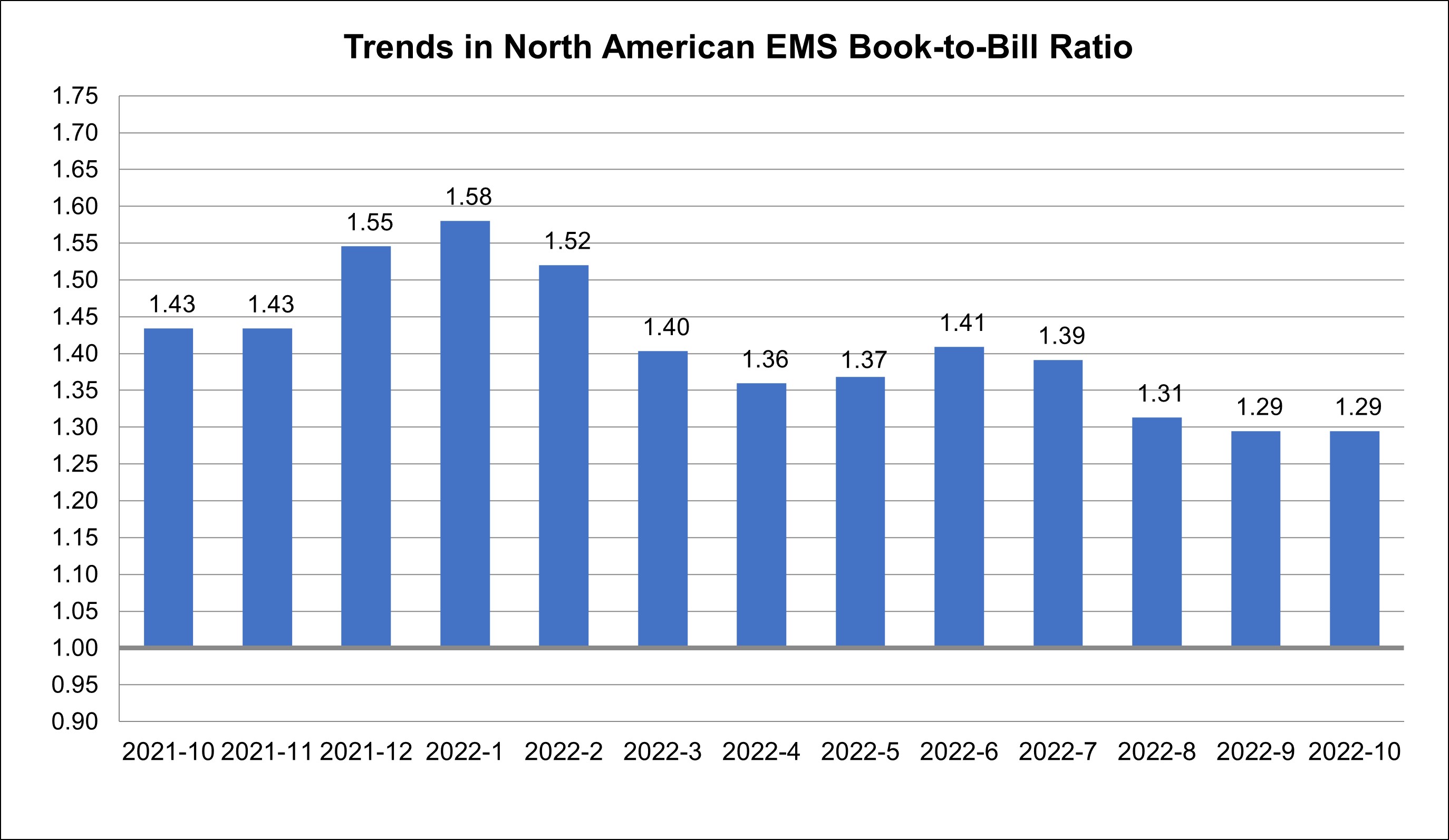
IPC announced today the October 2022 findings from its North American Electronics Manufacturing Services (EMS) Statistical Program. The book-to-bill ratio stands at 1.29.
Total North American EMS shipments in October 2022 were up 14.9 percent compared to the same month last year. Compared to the preceding month, October shipments decreased 2 percent.
EMS bookings in October increased 7.8 percent year-over-year and decreased 1.5 percent from the previous month.
“EMS orders and shipments remained above trend in October, despite a small reversal relative to last month,” said Shawn DuBravac, IPC’s chief economist. “Supply chain constraints have eased but shipment growth remains slightly constrained as some ongoing supply chain issues persist.”
Detailed Data Available
Companies that participate in IPC’s North American EMS Statistical Program have access to detailed findings on EMS sales growth by type of production and company size tier, order growth and backlogs by company size tier, vertical market growth, the EMS book-to-bill ratio, 3-month and 12-month sales outlooks, and other timely data.
Interpreting the Data
The book-to-bill ratios are calculated by dividing the value of orders booked over the past three months by the value of sales billed during the same period from companies in IPC’s survey sample. A ratio of more than 1.00 suggests that current demand is ahead of supply, which is a positive indicator for sales growth over the next three to twelve months. A ratio of less than 1.00 indicates the reverse.
Year-on-year and year-to-date growth rates provide the most meaningful view of industry growth. Month-to-month comparisons should be made with caution as they reflect seasonal effects and short-term volatility. Because bookings tend to be more volatile than shipments, changes in the book-to-bill ratios from month to month might not be significant unless a trend of more than three consecutive months is apparent. It is also important to consider changes in both bookings and shipments to understand what is driving changes in the book-to-bill ratio.
IPC’s monthly EMS industry statistics are based on data provided by a representative sample of assembly equipment manufacturers selling in the USA and Canada. IPC publishes the EMS book-to-bill ratio by the end of each month.