Key Summary
- The challenge: Across Teledyne's Machine Vision Camera Group sites in Europe and North America, workmanship decisions weren't consistent, as operators, inspectors, and engineers often interpreted "acceptable" differently, creating risk in high-reliability applications where training alone wasn't enough to close the gap.
- A common standard as the foundation: Through their partnership with the Global Electronics Association, the team made IPC Standards central to how quality is defined and communicated, turning them into a shared language for accept/reject decisions across every team and site.
- In-house certification at scale: By developing Certified IPC Trainers (CITs) internally and running IPC-A-610 J certification on-site, they accelerated onboarding, reduced reliance on external scheduling, and drove more consistent decision-making across shifts and locations with 24 team members certified in one recent cycle.
- Validation through the MIL Lab: Their Materials Interconnect Laboratory connects workmanship standards to measurable outcomes through ionic contamination testing (C3), dye-and-pull analysis, and cross-sectional analysis, enabling faster root cause analysis, stronger supplier feedback, and progress toward a 99.999% reliability goal.
- The payoff, internal and external: The integrated system of standards, training, and lab validation produced not only consistency on the floor but also customer confidence, reflected in praise from an aerospace and defense Global Quality Director during an audit and a subsequent multi-million-dollar contract award.
Here, we feature a real-world example of how electronics manufacturers are operationalizing quality at scale, written by members of our community who share their firsthand experience, thinking, and insights. In this piece, Cindy Tachihara and Cheewee Tng of Teledyne's Machine Vision Cameras Group walk through how they tackled workmanship consistency across multiple global sites, building a system that connects IPC Standards by the Global Electronics Association, in-house certification, and lab-based validation into a single, measurable approach to quality.
This is one way we seek to spotlight the practical work our members are doing every day: not theory or talking points, but the lessons, decisions, and turning points that come from actually building quality into a manufacturing operation. Our hope is that by sharing these stories going forward, others in the industry can learn from what's working, adapt it to their own environments, and continue raising the bar together.
Company Overview
Teledyne Technologies Incorporated (NYSE: TDY) provides advanced digital imaging products, instrumentation, aerospace and defense electronics, and engineered systems. Within Teledyne Vision Solutions, our Machine Vision Camera (MVC) Group manufactures imaging products across multiple sites in Europe and North America, with global sales support.
But like many electronics manufacturers, we operate in a fast-moving environment where quality and reliability depend heavily on consistent workmanship—and that’s something we’ve had to work hard to get right.
Where We Started: The Challenge of Consistency
A few years ago, we began noticing a familiar issue across our sites. Even with experienced teams, decisions about workmanship weren’t always consistent. Operators, inspectors, and engineers sometimes interpreted “acceptable” differently, especially as we brought in new employees with varying levels of experience.
This variability didn’t always show up immediately—but over time, it created risk. And in high-reliability applications, “almost consistent” isn’t good enough. We realized that training alone wasn’t solving the problem.
We needed a shared definition of quality that everyone—from the shop floor to engineering—could rely on.
What We Changed: Building Around a Common Standard
That realization led us to deepen our use of IPC standards through our partnership with the Global Electronics Association.
Instead of treating standards as reference material, we made them central to how we define and communicate quality. IPC standards became our common language, something every team could point to when making accept/reject decisions.
Just as importantly, we aligned our training programs to reinforce those standards in a structured, repeatable way. The goal wasn’t just certification, it was consistency in judgment.
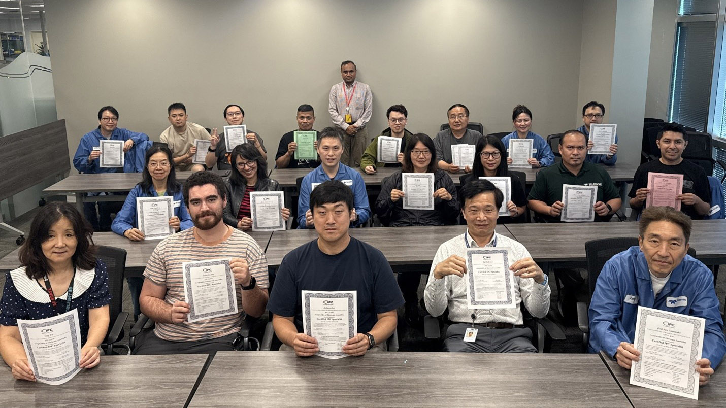
Scaling the Solution: In-House Training That Works
To make this sustainable, we invested in building internal capability.
We developed Certified IPC Trainers (CITs) within our teams and implemented in-house IPC-A-610 J certification. In one recent cycle, 24 team members completed certification (15 new and 9 recertifications).
This shift made a big difference. Instead of relying on external scheduling, we could train people faster, onboard new hires more effectively, and reinforce expectations directly in our production environment.
More importantly, we started to see more consistent decision-making across shifts, teams, and sites.
A Moment That Stood Out: Customer Validation
One of the clearest signals that we were on the right track came during a customer audit in the aerospace and defense sector.
During the audit, the Global Quality Director shared that, across hundreds of supplier audits, they rarely saw this level of alignment and professionalism with IPC-based standards.
Shortly after, we were awarded a multi-million-dollar contract.
That moment reinforced something we had been working toward: consistency isn’t just an internal goal—it builds real customer confidence.
Connecting Standards to Data: The Role of Our MIL Lab
Of course, standards and training are only part of the picture. We also needed a way to validate what we were seeing on the floor. That’s where our Materials Interconnect Laboratory (MIL Lab) comes in.
The lab allows us to connect workmanship standards to measurable outcomes through:
- Ionic contamination testing (Critical Cleanliness Control, or C3)
- Dye-and-pull analysis to verify solder joint integrity
- Cross-sectional analysis to uncover interconnect and plating issues
These tools have helped us move faster on root cause analysis and make more informed corrective actions. They also give us a way to provide clear, data-driven feedback to suppliers. Ultimately, this capability supports our broader reliability goal of 99.999%.
What We’ve Learned
Looking back, the biggest impact hasn’t come from any single initiative, it’s come from how everything works together.
- IPC Standards give us a clear definition of what “good” looks like
- Training and certification make that definition repeatable across people and teams
- Validation through the MIL Lab ensures those standards hold up in real production
Working with the Global Electronics Association has helped us bring these pieces together into a system that’s consistent, scalable, and measurable.
And for us, that’s been the real shift: moving beyond compliance to building a culture where quality is understood the same way, everywhere.