Alaska
- POPULATION (THOUSANDS) 733
- GDP (BILLION $) 70
- EMPLOYMENT (THOUSANDS) 472
- LABOR INCOME (BILLION $) 37
This interactive, virtual event will explain the main ways that cables and boards can act like antennas even though they're not designed to radiate. We'll discuss the two main radiating mechanisms and how they manifest in electronics hardware. Cables and split planes will get the most attention. We'll also include a live hardware demo that shows how these interactions play out in real life.
Building on the themes from my recent Community Magazine article, “Unlocking Workforce Potential: Beyond Federal Dollars,” this webinar will unpack how employers across the U.S. can access a range of underutilized funding opportunities to support training and apprenticeship programs. We’ll explore how national, state, and private resources can be braided to offset costs, expand training capacity, and build sustainable talent pipelines. While we’ll highlight recent examples—like the newly awarded Employment Training Panel (ETP) contract that supports California employers—our focus will be national, offering employers a practical roadmap for identifying, combining, and leveraging diverse funding sources to maximize workforce development impact.
This webinar explains how to use visual inspection alongside a plug-in thermal camera to detect circuit board faults. By spotting heat anomalies, engineers can quickly locate overheating components, shorts, or other issues that may not be visible — streamlining diagnostics and improving repair accuracy.
Join us for a practical, business-first approach to supply chain security. This webinar explores how involving non-IT stakeholders early in the process leads to smarter investments, fewer missteps, and clearer requirements for IT and security teams. Learn how to align security measures with business goals, avoid costly blind spots, and implement strategies grounded in the IPC-1792 white paper
Wire bonding remains the dominant chip-interconnection method—and it's not going anywhere soon. This webinar offers a practical overview of modern wire bonding processes, metrology challenges, and emerging materials. Learn about pitch shrinkage demands, direct bonding to Cu on ULK substrates, and innovations like silver and gold-coated palladium copper wires. Explore key bonding techniques including thermosonic, ultrasonic, and thermocompression, plus new options for Cu wire coatings.
Join SAE G19A subcommittee expert Anthony Bryant for an essential one-hour webinar focused on supply chain integrity and counterfeit electronics prevention. This session is specifically designed for non-technical personnel working in the electronics component supply chain including procurement professionals, supply chain managers, quality assurance staff, and business leaders.
This webinar, titled "Electronic Essentials: What You Think You Know - and More", is a foundational session aimed at reinforcing the core knowledge that every technician, inspector, assembler, operator, and engineer in electronics manufacturing should possess. These are the essentials of quality and reliability in electronics manufacturing—the things you should know without flipping through an IPC standard. Whether you're new to the field or a seasoned pro, this session is your checklist for baseline competency. Knowing these terms without referencing IPC standards demonstrates professional readiness and process awareness and supports faster troubleshooting, better communication, and supports a better team culture.
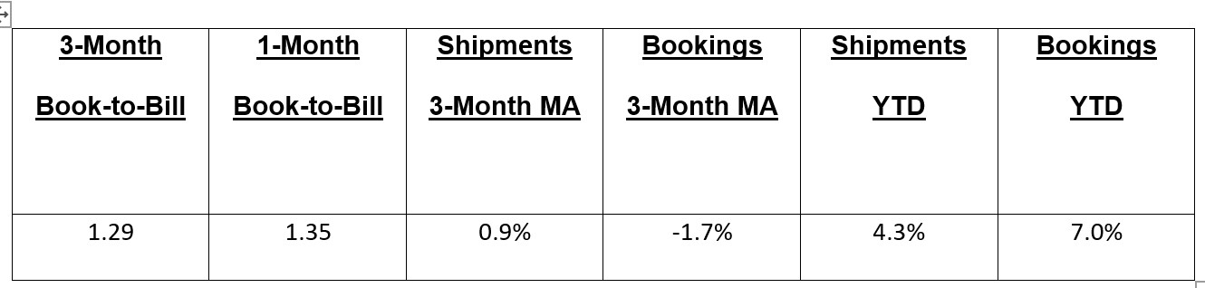
The Global Electronics Association announced today the March 2026 findings from its North American Electronics Manufacturing Services (EMS) Statistical Program. The book-to-bill ratio stands at 1.29.
Total North American EMS shipments in March 2026 were up 6.9% compared to the same month last year. Compared to the preceding month, March shipments were up 5.3%. March’s year-to-date (YTD) shipments increased by 4.3% year-over-year (YOY).
EMS bookings in March decreased 1.7% year-over-year and increased 7.0% from the previous month. March’s YTD bookings increased by 0.6% compared to the same period last year.
“The EMS industry posted a solid March, with shipments up for the fourth consecutive month. Customer demand looks sustained headed into the second quarter,” said Dr. Shawn DuBravac, Global Electronics Association’s chief economist.
Detailed Data Available
Companies that participate in the Global Electronics Association’s North American EMS Statistical Program have access to detailed findings on EMS sales growth by type of production and company size tier, order growth and backlogs by company size tier, vertical market growth, the EMS book-to-bill ratio, 3-month and 12-month sales outlooks, and other timely data.
Interpreting the Data
The book-to-bill ratios are calculated by dividing the value of orders booked over the past three months by the value of sales billed during the same period from companies in the Global Electronics Association’s survey sample. A ratio of more than 1.00 suggests that current demand is ahead of supply, which is a positive indicator for sales growth over the next three to 12 months. A ratio of less than 1.00 indicates the reverse.
Year-on-year and year-to-date growth rates provide the most meaningful view of industry growth. Month-to-month comparisons should be made with caution as they reflect seasonal effects and short-term volatility. Because bookings tend to be more volatile than shipments, changes in the book-to-bill ratios from month to month might not be significant unless a trend of more than three consecutive months is apparent. It is also important to consider changes in both bookings and shipments to understand what is driving changes in the book-to-bill ratio.
The Global Electronics Association’s monthly EMS industry statistics are based on data provided by a representative sample of assembly equipment manufacturers selling in the USA and Canada. The Association publishes the EMS book-to-bill ratio by the end of each month.