EMSCO: Where Membership, Craftsmanship, and Community Converge
Key Summary:
EMSCO showcases strong U.S. manufacturing through a people-centered, high-quality production model built on flexibility, craftsmanship, and accountability.
Membership matters: EMSCO says its engagement with WHMA and the Global Electronics Association has helped inform its leadership, operations, and long-term growth.
Policy engagement is also key, as Congressman Rob Wittman’s visit highlighted the importance of connecting policymakers with shop-floor manufacturing realities.
At EMSCO, value isn’t created in conference rooms, it’s built on the production floor. That philosophy, often described by the Japanese concept of Gemba, “the real place,” comes to life the moment you step inside the company’s Ashland, Va. facilities. What makes EMSCO particularly compelling is how they build, and how their engagement with the Global Electronics Association and WHMA has helped shape what they’ve built.
Building with Purpose on the Production Floor
EMSCO’s operation reflects a deliberate commitment to craftsmanship, flexibility, and people. In its newer facility, the company is tackling a complex, large-scale project: hydroponic lighting assemblies for a first-of-its-kind indoor strawberry farm. These 35-foot “spines,” engineered for decades of reliability, integrate power, harnessing, and structural components into a single system. When the customer lacked a method to move these multi-ton assemblies, EMSCO engineered its own, demonstrating the kind of IDEO “how might we” problem-solving that defines the company.
A Culture Built to Last
That same mindset extends across the organization. EMSCO operates with a “one harness, one person” philosophy: Builders own the process from start to finish, including cutting, assembly, testing, and shipment. The result is not just efficiency, but accountability and pride. Combined with a highly flexible production environment featuring modular, self-designed workstations and mobile equipment, EMSCO can adapt quickly to changing customer needs without sacrificing quality.
Underlying this operational model is a deeply intentional culture. EMSCO has maintained near-zero turnover for over a decade, investing in cross-training and promoting from within. Employees regularly expand beyond their initial roles, gaining experience in engineering, accounting, and production. This approach reinforces a workplace where people are trusted, challenged, and directly connected to the value they create.
Strength Through Association
Critically, EMSCO’s evolution has not happened in isolation. The company’s long-standing involvement with WHMA, and, more broadly, the Global Electronics Association, has played a meaningful role in shaping its leadership philosophy and strategic direction.
EMSCO President Parker Garrett and WHMA Board Chairman, views membership not as a credential, but as a learning network. Through years of engagement, he has built relationships with industry peers, visited dozens of manufacturing operations, and exchanged ideas that later informed EMSCO’s own practices, from shop-floor design to leadership approach. These connections provided real-world insight into what works, and what doesn’t, across the industry.
That exchange of knowledge is a defining benefit of Association membership. For EMSCO, it has translated into tangible operational decisions and a clearer vision for growth. Rather than pursuing scale for its own sake, the company has remained intentionally right-sized, prioritizing culture and cohesion over complexity, an approach reinforced through conversations with fellow members facing similar challenges.
The Power of Staying Connected
Today, EMSCO continues to grow through referrals and long-term partnerships, not transactional sales. The company regularly turns down opportunities that don’t align with its values, focusing instead on customers who view them as collaborators rather than commodity suppliers.
EMSCO’s story is a reminder that strong companies are not built in isolation. They are shaped through shared experience, continuous learning, and meaningful industry connections. For members of the Global Electronics Association and WHMA, that ecosystem is one of the most valuable assets available.
At EMSCO, the results speak for themselves: when you stay close to the work, be actively involved in your industry association and connected to your industry, you build more than products. You build a company that lasts.
On the Floor with Policymakers: Congressman Wittman Visits EMSCO
On April 27, Congressman Rob Wittman visited EMSCO’s Ashland, Va. headquarters for a firsthand look at the company’s wire harness and printed circuit board assembly operations.
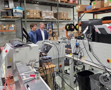
Wittman, known for his focus on reshoring U.S. manufacturing and advancing STEM and career and technical education, met with employees across the facility and discussed the role of interconnect technologies in modern electronic systems.
The Congressman also highlighted several legislative efforts aimed at strengthening domestic manufacturing and supply chain resilience, including the Finding ORE Act (H.R. 2969), which supports cooperation on mapping critical minerals and rare earth elements, and H.R. 7126, which proposes the establishment of a U.S. Strategic Resilience Reserve.
EMSCO President Parker Garrett noted that policies supporting material availability and supply chain stability are critical to long-term planning. Greater cost predictability, he said, would enhance the competitiveness of U.S. manufacturers in the global market.
The visit underscored the importance of connecting policymakers with shop-floor realities, an ongoing priority for manufacturers navigating workforce, supply chain, and competitiveness challenges.