Key Summary
• White House announced over $5B in expected CHIPS R&D investments, including major workforce funding
• NSTC formally launched as a public-private consortium, alongside expanded roles for NatCast
• John Mitchell represented IPC, emphasizing a workforce strategy spanning “silicon to systems”
• IPC highlighted scalable career pathways using industry-recognized credentials
• Federal leaders reinforced the urgency of building a large, skilled workforce to support CHIPS initiatives
Today at the White House, leaders from the Departments of Commerce, Defense, and Energy; the National Science Foundation; and the National Center for the Advancement of Semiconductor Technology (NatCast) gathered for an event to announce more than $5 billion in expected investment in the CHIPS R&D program. The announcement includes hundreds of millions of dollars of expected investment in the semiconductor workforce and funding announcements in packaging, metrology, and a CHIPS Manufacturing USA Institute. It also formally establishes the National Semiconductor Technology Center (NSTC) as a public-private consortium.
View NIST’s full press release here.
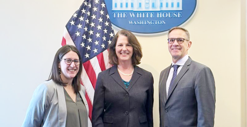
IPC’s President and CEO, Dr. John W. Mitchell, participated in this commemorative signing, as well as a White House CHIPS R&D Roundtable that followed. This occasion marks a significant stride towards strengthening the nation's technological leadership. As we extend our heartfelt congratulations to NatCast and NSTC, we are excited to share the positive outcomes of this landmark event that promises to shape the future of the industry.
NatCast and NSTC are set to play pivotal roles in advancing semiconductor technology, fostering innovation, and bolstering the nation's tech leadership. NatCast will focus on pushing the boundaries of semiconductor technology, while NSTC will serve as a hub for collaborative research and development initiatives. We extend our congratulations to the teams behind NatCast and NSTC.
After the signing, John was asked to join the Director of the National Science Foundation, and leadership from the Departments of Labor and Commerce, along with panel of experts across industry, academia, and nonprofits to offer perspective on how the CHIPS R&D program can build the workforce needed to make the CHIPS investments successful. During the roundtable discussions, John shared pointed insights on behalf of the electronics manufacturing industry.
Highlights of John’s comments shared today:
- We can’t solve the workforce problem for slices of the industry. Building a “semiconductor” workforce is an inherently flawed notion. We need a robust workforce from “silicon to systems.”
- Creating career pathways is key. IPC and industry partners have built career pathways via portable, stackable, industry-recognized credentialing. In an industry as marginalized by government as electronics, greater federal support is welcome.
- Real impact means scale and speed. For the CHIPS for America program to succeed, America will need hundreds of thousands more skilled workers in this decade, not just in chips but in related sectors as well.
Deputy Secretary of Defense Kathleen Hicks remarked, “We [at the Pentagon] know that the research and development on semiconductors and microelectronics helps us to make sure that we can actually develop and manufacture at the cutting edge.”
Dr. Laurie E. Locascio, Under Secretary of Commerce and Head of the National Institute for Standards and Technology (NIST), highlighted the strategic need to develop our workforce when she said, “We have to consider how we are going to develop the people who will take these jobs. We need to create programs to support the development of enough inventors and designers, and researchers, and developers, and engineers and technicians to meet the government needs and the needs of this growing and wonderful commercial sector. And we have to ensure that these investments build upon each other toward a strengthened ecosystem -- which is what we’re trying to achieve in the United States.”
Today was about marking a major milestone on the path to building a strong and resilient industry. It was also an opportunity to engage in substantive dialogue about how we can make real and lasting impact in solving the challenge of building the strong workforce needed to power and lead industry forward. IPC is honored to have had the opportunity to contribute to that discussion, and we look forward to continued partnership and collaboration.